
by Chris Font on Aug 10, 2017 10:00:00 AM
We all encounter things that have a way of mildly frustrating us. Enough to bug us, but just not enough to go out of our way to correct. It could be a sticky lock in desperate need of a spray of WD-40, a weed growing in the middle of the sidewalk, or a dusty tabletop. For some time this annoying thing for me was a coat closet in the middle of the house without any light in it. Having two dogs that sometimes forget shoes are not chew toys, this closet has become the convenient home to our shoe collection. As time went on more shoes accumulated and the second law of thermodynamics held true – the closet became a dark, disorderly mess.
I have wanted to take a stab at etching a PCB for some time. This seemed like the perfect opportunity to test out this new method. The circuit would not be complicated so I could also shine some light on others (as well as my closet) who may be considering this for the first time.
Step 1: Sketch a Schematic and Check the Math
This project in particular requires LEDs, resistors, a switch and some type of battery. The goal is to use a normally closed switch to keep the LEDs off when the door is shut and to turn them on once the door is opened. Sketch out a circuit and track down all required components. Be sure to do your Ohm’s Law check to make sure all parts are sufficiently rated. In my case, I found the current going through each LED on fully charged 18650 cell (my battery of choice) would be a tad high. However, I decided to continue with this set up to prevent the LEDs from getting too dim as the cell dies. Plus, I had a plethora of 100 Ω resistors leftover from a previous project that were just waiting to have a purpose! Circuit design and component selection are foundational engineering activities that support larger system designs developed through professional engineering services.
.
Step 2: Input your Design into a PCB Design Software
Using a decent PCB Design platform can save a lot of time while designing the layout of your PCB. Programs such as Eagle and EasyEDA allow you to design your schematic then build directly from this schematic. This ensures component sizes and connection points are accurate and accounted for on the PCB. Another timesaver of this software is the autorouter tool. This will lay out all traces in paths that only interfere with components and other traces that are connected. After the PCB has been laid out and the circuit connections have traced, verify the circuit one final time prior to printing. Make sure to print using a 1:1 scale so the layout dimensions are accurate.
Step 3: Transfer the Layout to the Board
To ensure an accurate transfer, tape this print out over top of a copper clad laminate PCB. Using a pushpin, stab through the paper where each component lead will penetrate the board. This will leave dots on the copper where these components go. The small indentation on the copper will also help the drill bit find the exact location the lead will go. Remove the printed sheet and make sure all components are marked on the copper. Use a 1/32” (maximum) bit to drill out the holes that were marked on the board. Once all the holes are drilled, clean the top of the copper plate with a piece of sandpaper. Using a permanent marker, draw to traces between all the components referencing the printed PCB layout. Allow some time for the ink to dry and touch up the board where the marker is faint.
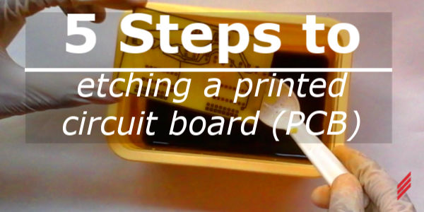
Step 4: The Etching Process
Once the second coat of marker is completely dry it is time to give the board a bath in ferric chloride. Ferric chloride is a corrosive, acidic chemical compound that will eat away all copper on the board that is not protected by the marker’s ink. Pour a modest amount of ferric chloride into a plastic container with a lid; just enough to cover the board completely. Let the board soak for 10 minutes, make sure the lid is properly secured and agitate it every few minutes by rocking the container back and forth. After 10 minutes inspect the board and if no copper is visible, remove the board while wearing a latex glove. Pat the board dry with a disposable rag to remove all ferric chloride from the board. Rinse the board with acetone that will make quick work of the marker ink to reveal your unharmed traces. The etching process is complete!
Step 5: Populate the Board and Test Your Circuit
After the board has been etched, use a multimeter to do a continuity test. Make sure all traces were successful and also begin and terminate in the correct locations before applying power to the circuit. Once all traces have been verified, add the components to their correct position and solder them in. Apply voltage and watch in awe as your perfectly etched circuit functions exactly as planned!
My Next Step
To complete my project I will attach the 18650 holder to the backside of the PCB and mount the assembly inside my closet. The switch has normally closed contacts so that when the door is closed the switch will be pressed, the contacts will be open, and the lights will be off. When the door is opened the switch will not be pressed, the contacts will be closed and the light will be on!
About the author
Chris Font has left Hallam-ICS to pursue other endeavors, but his contributions to the company continue to be valued.
Read My Hallam Story
About Hallam-ICS
Hallam-ICS is an engineering and automation company that designs MEP systems for facilities and plants, engineers control and automation solutions, and ensures safety and regulatory compliance through arc flash studies, commissioning, and validation. Our offices are located in Massachusetts, Connecticut, New York, Vermont and North Carolina and our projects take us world-wide.


Advancing Automation Technology - How to Specify a KVM Console

Partners

Comments (1)